This assignment consists of a one larger project. The objective is to expose you to the process of building a complete system from smaller pieces. As in software engineering, you'll have some modules already available and will have to learn how to use them. There will be only be two modules that you will have to complete. Their interfaces are already defined. All other modules will already be complete.
A receiver modules is provided for you as an example and a test bench. It receives the serial data and extracts and destuffs the data. It uses four hex displays to show the data it has received. It also checks that the packet is the right length and that the check sum is correct. Both LenOK and ChkOK are only valid when PktRcvd is high. The receiver module is a sub-circuit that is decomposed in a similar way to the transmitter you will be constructing. Use it is as a case study and as a Verilog style guide.
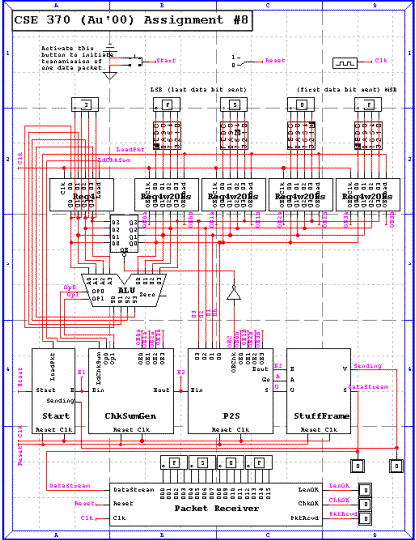
To begin, download the project files. Unzip the file on the C: drive so that in the end you have a folder C:\assignment8. This will guarantee that all the Verilog modules in the project will maintain their links to their Verilog source (it has to be in a folder with this name because of DesignWorks's insistence on absolute rather than relative path names). Start up DesignWorks by double-clicking on the design C:\assignment8\a8.cct which is the high-level block diagram of the project and its test bench. Just click "OK" in the Invalid Directory dialog box that will pop when DesignWorks is unable to locate its standard libraries in that directory. Once the design is open, go to the "Parts" window and open a8.clf by clicking the right button and selecting "Open...". You should now have all the modules used in this design visible in the "Parts" window.
Make sure to take some time to look at all the internals of all modules provided. For this assignment, it is critically important that you understand the function of each of the modules not just the ones you will be completing.
The component at the bottom of the drawing sheet (labelled Packet Receiver) is the test bench. At the top of the drawing sheet, you will find four hex keypads you can use to set the data contents of your packet. There are five hex displays that show the data (mirroring the four hex keypads) and the checksum (after it is computed and placed in the check sum register). A push button switch is provided to indicate to the circuit to start sending a packet. There is also a reset switch to be used only at the beginning of your simulation (your circuit should be able to transmit multiple packets without needing to be reset).
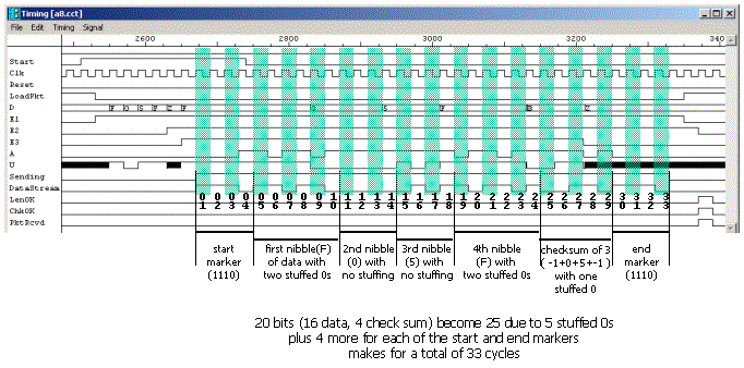
To begin open up the "simulator" tool and the "timing" tool. You should see some signals in the timing window (these are the inputs and outputs of the four sub-modules of your design as well as the outputs of the packet receiver module). Start the simulator and set the reset switch high for at least one clock cycle. Set the data of the packet to be hex F05F from right to left (note that the most significant bit is on the right). Now, hold down the "Start" push button for at least one clock cycle and you'll see how the "Start" module generates LoadPkt and E to get the ball rolling for the following module.
Below is a drawing that shows how the timing window should look once you've completed your assignment. Note how the ChkSumGen module computes the checksum and places it in the check sum register (you can see the data values on the data bus). The P2S module serialized the data and presents it (as needed) to the StuffFrame module. The StuffFrame module is almost identical to the finite state machine you constructed for the problem #3 of assignment #7. It just has one extra output to indicate when the output is valid (V). This valid output is used to indicate that the transmitter is sending while the S output is the data being transmitted. The Sending signal is used to indicate to the Start module when the packet has been completely transmitted so that it can reset get ready for the next press of the start button (this guarantees that we do not try to start another packet while one has yet to finish). Note that there are 33 bits for the packet with data 16'hF05F. The packet consists of these 16 bits, 4 bit checksum, 5 extra bits used to stuff the data, and 4 bits each for the start and end markers.
Your task is to design the ChkSumGen and P2S modules. These two finite state machines control the ALU used to compute the check sum, the check sum register load signal, and the data bus. Note that the ALU can perform pass, add, and subtract operations. The check sum register can be used as an accumulator for the addition of the four data nibbles. All other modules besides ChkSumGen and P2S are already complete and should NOT be altered. You will only need to edit the internals of the Verilog files for the ChkSumGen and P2S modules.
The transmitter modules
The Start module's function is to indicate when a packet should be transmitted and to load up the data registers. It waits until the packet has been completely sent before allowing another packet to begin (by observing the Sending signal).
The ChkSumGen module routes the data values into the ALU so that it can accumulate a check sum in the check sum register.
The P2S module serializes the data and check sum by reading them in turn from the five registers at the top of the drawing. It also can hold up the data stream based on the value of its Go input (connected to the advance (A) output of the StuffFrame module).
The StuffFrame module transmits the packet by enclosing the serial data provided by the P2S module within start and end markers and bit stuffing the data so that the pattern of the start and end markers does not occur in the data payload.
The receiver modules
The Framer state machine's function is to determine the start and end of the packet data stream. This machine includes a pattern detector and a shift register.
The Destuffer state machine's function is to determine that the length of the packet is correct (20 bits = 16 payload + 4 checksum) and signal which 0s are stuffing and to be ignored downstream. This machine includes a counter.
The S2P state machine's function is to transform the serial data to parallel format and load it into the registers of the data path. Note that this machine includes a shift register.
The Chksum state machine's function is to take each nibble through the ALU and accumulator to determine whether the check sum is correct. It uses several of the ALU's functions including subtract for the final comparison. This machine also signals that a packet has been received and whether its checksum and length are correct.
Make sure that your machines are designed so that they only need to be reset once at the beginning and not after every packet.
Extra Credit:
Come up with circuit realizations for the two modules. Create two new modules (ChkSumGenSch and P2SSch), place them in your drawing, attaching internal subcircuits with your FSM schematics, and simulate the circuit again. Turn in schematics and simulation waveforms. This will add 25% bonus points to the grade of this assignment.)
Have fun!