
Each problem is on a separate sheet of paper. Write your answer neatly in the space provided. If you need more space (you shouldn't), there are a couple of extra sheets at the end of the exam, but please make sure that you indicate clearly the problem to which the comments apply. Do NOT use any other paper to hand in your answers.
The exam is CLOSED book and CLOSED notes. Please do not ask or provide anything to anyone else in the class during the exam. Make sure to ask clarification questions early so that both you and the others may benefit as much as possible from the answers.
Good luck.
Name:
ID#:
|
Problem
|
Max Score
|
Score
|
|
1
|
15
|
15
|
|
2
|
20
|
20
|
|
3
|
25
|
25
|
|
4
|
40
|
40
|
|
TOTAL
|
100
|
100
|
1. Boolean Algebra (15 points)
In many places there is a general rule that shellfish should only be eaten in months with an "R" (i.e., January, February, March, April, September, October, November, and December). Given a code for the month with January = 0001 and December = 1100 (note that 1100 = m8 m4 m2 m1 with m8 = 1, m4 =1, m2 = 0, and m1 = 0) complete the Karnaugh below for the Ivar function which is true if the month has an "R" in it and false otherwise. (Note: Ivar is a contraction for "I have an R" as well as a reference to Seattle's beloved Ivar Heglund.)
(a) Complete the map. Make sure to consider don't cares.
(b) List ALL the prime implicants for this function.
m8'm2'm1', m4m2'm1', m8'm4', m8m4, m8m1, m8m2, m4'm1, m4'm2(c) Of the list for part (b), which are essential prime implicants?
none are essential(d) Derive a minimal sum-of-products expression for this function.
m4m2'm1' + m4'm2 + m4'm1(e) Using exactly the circuit shown below, connect m8, m4, m2, and/or m1 to the inputs so that the output is the Ivar function.
The expression above can be rewritten as: m4(m2 + m1)' + m4'(m2 + m1) = m4 xor (m2 + m1)

(f) Verify your work for part (e) by using the axioms/theorems of Boolean Algebra to show that the expression for Ivar from the circuit schematic is equivalent to the expression you derived for part (d). You may or may not have to use don't care information to show this equivalence.
m4m2'm1' + m4'm2 + m4'm1
m4(m2 + m1)' + m4'm2 + m4'm1 (de Morgan's)
m4(m2 + m1)' + m4'(m2 + m1) (distributive)
m4 xor (m2 + m1) (XOR definition)
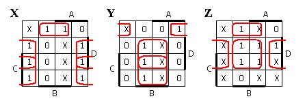
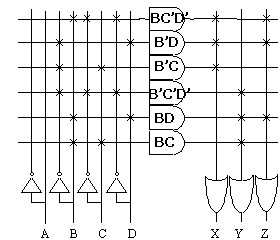
2. Programmable Logic (20 points)
Given three Karnaugh maps for the functions for X, Y, and Z, implement them using the 4 input, 3 output, 6 product term PLA shown below. Personalize the PLA by placing an X at the appropriate intersection where you want a connection to be made. Also, write the product term implemented on each row of the AND plane inside the AND gate that forms that term.
Minimizing each function in isolation would require a total of 8 different product terms.X = BC'D' + B'D + B'CThe crucial step for this problem is to not minimize Z in isolation but to realize that it can reuse implicants from X and Y.
Y = B'C'D' + BD + BC
Z = BC' + DZ = BC'D' + B'D + BD
3. Timing (25 points)
(a) In the data path shown below, there are five paths of three different lengths between registers. Assume that the registers have setup/hold/propagation times that are 3/2/4, the tristate drivers have a delay of 6, and the ALU has a delay of 12, what is the critical path of this circuit and what is the fastest (smallest cycle time) at which we can run this datapath? Clearly describe the critical path by naming the starting register, all combinational logic and busses through which the register output will pass, and the ending register (e.g., C, through ALU, back to C).

The critical path (the one with the largest delay between registers) starts from RegA (or RegB), goes through the tri-state driver, onto the data bus, through the ALU, and ending at the input to RegC. The delay is:(b) A designer has modified the data path by adding another register. What is the new critical path and what is the new fastest cycle time?prop time of FF + delay of tristate driver + delay of ALU + setup time of FF
= 4 + 6 + 12 + 3 = 25Thus, the shortest clock cycle at which this circuit will function correctly is 25 time units.
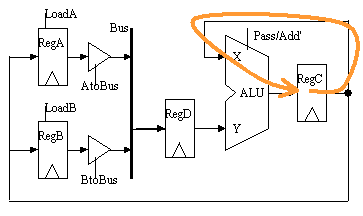
The critical path now starts from RegC goes through the ALU, and ending back at the input to RegC. The delay is:(c) The technique used to speed up the circuit above is called pipelining. What implications does it have for how this data path can now be used by a finite state controller?prop time of FF + delay of ALU + setup time of FF = 4 + 12 + 3 = 19Thus, the shortest clock cycle at which this circuit will function correctly is 19 time units.
Completing some data operations between RegA (or RegB) and RegC now take two cycles instead of one. A controller implementing an add operation would now need an extra state for that instruction. Although this will make all clock cycles faster (19 instead of 25 time units), it may not improve overall performance due to the extra states some operations will require to use the ALU.
4. Finite State Machines (40 points)
(a) Given the state diagram below for an asynchronous Mealy machine, a former CSE370 student came up with the following Verilog code to describe it. Are there any non-syntactic errors with the Verilog description? If so, state them clearly with numbered sentences to describe each error and what effect it would have on the simulation, if any.
module unknown (clk, reset, in, out);
  input     clk, reset, in;
  output    out;
  reg       out;
  reg [3:0] state; // state variable
`define A 4b0000 `define B 4b0001 `define C 4b0011 `define D 4b0111 `define E 4b1111
  always @(posedge clk) begin
    if (reset) begin out = 0; state = `A; end
    else
      case (state)
        `A: if (in) state = `B; else state = `A;
        `B: if (in) state = `C; else state = `A;
        `C: if (in) state = `D; else state = `A;
        `D: if (in) begin out = 1; state = `E; end else state = `A;
        `E: if (in) state = `E; else state = `E;
     endcase
  end
assign out = state[3];
endmodule
(b) Generate a Verilog description of the same state diagram implemented
as a synchronous (or registered) Mealy machine. Use the same state
encoding as in the Verilog provided in part (a).
(c) Implement your state machine using the shift register component provided below. Use whatever additional combinational gates and/or flip-flops you feel are necessary. Try to realize the most efficient (fewest other parts) circuit you can devise.module unknown (clk, reset, in, out); input clk, reset, in; output out; reg out; reg [3:0] state; // state varable `define A 4b0000 `define B 4b0001 `define C 4b0011 `define D 4b0111 `define E 4b1111 always @(posedge clk) begin if (reset) state = `A; end else case (state) `A: if (in) state = `B; else state = `A; `B: if (in) state = `C; else state = `A; `C: if (in) state = `D; else state = `A; `D: if (in) state = `E; else state = `A; `E: if (in) state = `E; else state = `A; endcase end always @(state or in) begin out = 0; if ((state == `D) & (in)) out = 1; if ((state == `E) & (in)) out = 1; end endmodule

module shifter (Clk, Clear, LeftIn, RightIn, Enable, Direction, Q0, Q1, Q2, Q3);
  input     Clk, Clear, LeftIn, RightIn, Enable, Direction;
  output    Q0, Q1, Q2, Q3;
  reg       Q0, Q1, Q2, Q3;
  reg [3:0] data;
always @(posedge Clk) begin
if (Clear) data = 4b0000;
else
if (Enable) begin
if (Direction) data = {LeftIn, data[3:1]};
else data = {data[2:0], RightIn};
end
end
assign Q0 = data[0];
assign Q1 = data[1];
assign Q2 = data[2];
assign Q3 = data[3];
endmodule
Direction = 0
Enable = in (or, alternatively, 1 since the register is cleared when in = 0)
RightIn = 1
LeftIn = X
Clear = reset + in'
Clk = clk
Out = Q3
