CSE370 Assignment 6
Design Works Project
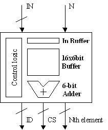
Implement a circuit that receives as input 6-bit values and performs
the following functions:
- Maintains a sorted list of the last 16 input values
- Outputs the "Nth element" of the list, where "N" is a 4-bit input
- Provides a 6-bit checksum "CS" of the elements in the list
- "CS" is obtained by 6-bit addition of list elements,
where the more significant bits/carry-out are discarded
- Resets all list values to zero when input equals 101010 (thus the list
never contains 101010 as an input value)
The circuit must have exactly one 6-bit adder. You are allowed to use
incrementers freely. If your circuit requires X cycles to perform all functions,
assume your input arrives at exactly X cycles.
In your design, strive for clarity, ease and correctness of implementation.
In addition to the schematics, create a test vector that clearly
drives the full functionality of your design. Produce the
corresponding timing diagram and mark on it the phases that exercise
each function and when the results of that phase become available.
Additional requirements and suggestions
Your circuit must follow the naming conventions for inputs and outputs as follows:
- the 6 bits of the input value must be named
InValue0 ... InValue5
- the 4 bits of the index input must be named
InIndex0 ... InIndex3
- the 6 bits of the Nth Element output must be named
NthElement0 ... NthElement5,
- the 6 bits of the Check Sum must be named
Checksum0 ... Checksum5,
- the 1 bit of the clock input must be named Clock
(this only applies if you use Test Vector to produce clock signals)
In all cases (except Clock) the bit numbered 0 is the least
significant bit, and the bit numbered 5 (or 3 for the index input) is
the most significant bit.
Unless you turn in a completely working implementation, you may
improve your grade by turning in a short (but clear!) writeup containing:
- the status of your implementation, including which functions you
have implemented
- a high-level description of the structure of your design, briefly
explaining how you implemented each function
- the finite-state machine that controls your circuit, including the
conditions to transition from state to state
- specification of how many clock cycles the circuit takes to compute the outputs and when it reads the inputs
Turn-in instructions
You will need to turn in the following:
- all circuit and part library files necessary to load your design in DesignWorks
- your test vector file
- the write-up (optional)
The writeup is to be submitted on paper at beginning of (or before) the final.
The files are to be submitted electronically as follows (see Notes below):
Note 1. Turnin will be enabled on Wednesday 3/14.
Note 2. If you are unfamiliar with using UNIX servers, you are allowed to email the project.zip file to vass@cs.washington.edu. Please do NOT email it until Wednesday afternoon. You should also be available right after the final exam to re-send the file if we have not received it.
Comments to: cse370-webmaster@cs.washington.edu
(Last Update: )