CSE370 (Autumn 03) Assignment 7 Solution
1. Write a behavioral Verilog module for the circuit of exercise 5 in the previous assignment and simulate it for the same conditions. Turn in the Verilog code and the simulation waveforms.

2. CLD-II,
Chapter 7, problem 7.3
7.3 Consider the design of a 4-bit BCD counter that counts in the following sequence: 0000,0001,0010,0011,0100,0101,0110,0111,1000,1001, and then back to 0000.
a.
Draw the state diagram and state transition table.
|
|
|

b.
Implement the counter using D flip-flops.
|
|
|
|
|
|


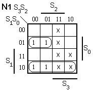

N3 = S3•S0’+S0•S1•S2
N2 = S0•S1•S2’+S0’•S2+S1’•S2
N1 = S0•S1’•S3’+S0’•S1
N0 = S0’

c.
Implement the counter making it self-starting.
The minimizations for
part b leave a self-starting counter.
|
|
|

3. CLD-II, Chapter 7, problem 7.9
7.9 Use two cascaded synchronous up-counters to implement a 6-bit offset counter that counts from 000010 to 110011 and repeats. Make sure the counter begins in state 000010 when the external reset signal is asserted.

4. Chapter 7, Problem 7.11
7.11 Consider the design of a bit-serial adder. This circuit uses a single full adder to add two binary numbers presented in serial fashion, 1 bit at a time.
a. Draw the schematic for a 4-bit version of this circuit. Two 4-bit shift registers are loaded with the data to be added in parallel. These are shifted out a bit at a time, starting with the lowest-order bit, into the A and B inputs of the full adder. The partial sum is shifted into a third register. How should the carry out be handled between subsequent bits?

b. Define your control signals for the bit-serial adder subsystem. Draw a timing diagram that illustrates the sequencing of these signals to implement the 4-bit addition. What happens on reset?

On reset, the DFF that stores
the Carry out must be set to 0. All other values are overwritten when LD is
asserted.
5. CLD-II, Chapter 7, problem 7.12
a. Design a system that will generate a single clock pulse one period long each time a push-button is pressed. (you may assume an external reference clock is available.)

Note: This circuit will generate a pulse slightly longer than the duty cycle of the reference clock. It still generates only 1 pulse even if the button is held down.
b. Design a system using a ‘163 counter that will assert a signal for exactly 13 clock pulses each time a push-button is pressed. (Assume a reference clock is available.

c. Design a circuit that will generate a single clock pulse each time a STEP push-button is pressed. Provide a separate circuit, independent of STEP that will cleanly turn the clock on when a RUN switch is in the ON position and off when RUN is in its OFF position. No marginal/partial clock outputs are allowed.

6. CLD-II, Chapter 7, problem 7.15
7.15 Redesign the odd parity checker FSM of Section 7.2.1 to make it check for even parity ( that is, assert the output whenever the input contains an even number of 1s). Show your state diagram.
|
|
|
