Each problem is on a separate sheet of paper. Write your answer neatly in the space provided. If you need more space (you shouldnt), there are a couple of extra sheets at the end of the exam, but please make sure that you indicate clearly the problem to which the comments apply. Do NOT use any other paper to hand in your answers.
The exam is oepn book and notes. Please do not ask or provide anything to anyone else in the class during the exam. Make sure to ask clarification questions early so that both you and the others may benefit as much as possible form the answers.
Good luck.
Name:
ID #:
|
Problem
|
Max Score
|
Score
|
|
1
|
10
|
|
|
2
|
25
|
|
|
3
|
15
|
|
|
4
|
25
|
|
|
5
|
25
|
|
|
TOTAL
|
100
|
1. Combinational Logic (10 points)
You are to design a circuit that takes a 4-bit number as input (I8, I4, I2, I1) and generates an output which is 1 if the input number is one of the prime numbers between 0 and 15 inclusive. You may assume that the input is never 0, 1, or 2. The most significant bit of the input is I8. Please use the Karnaugh map below for this problem.
(a) Write this function as a list of
minterms
(S
notation).
S m(3, 5, 7, 11, 13) + d (0, 1, 2)
(b) List the prime implicants
for this function.
I8'I4', I8'I1, I4I2'I1, I4'I2I1
(c) List the essential prime
implicants for this function.
I8'I1, I4I2'I1, I4'I2I1
(d) Find the minimal sum of
products expression for this function.
I8'I1 + I4I2'I1 + I4'I2I1
(e) Draw a circuit diagram
for the mimized function using only AND, OR, and NOT gates.
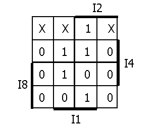
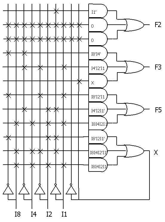
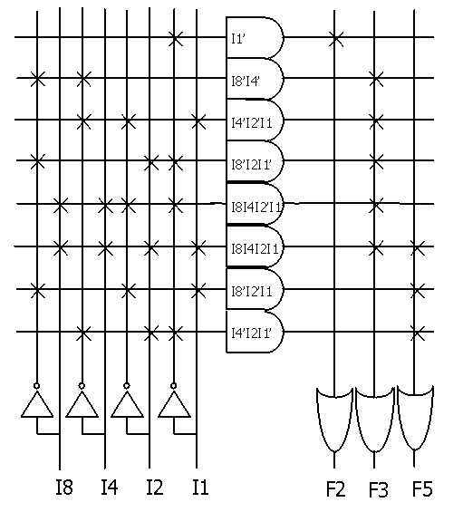
2. PAL/PLA/ROM Implementations of Combinational Logic (25 points)
You are to implement three functions
(F2, F3, F5) of the same input (I8, I4, I2, I1 as in the problem above)
that indicate when the binary is divisible by 2, 3, and 5, respectively.
Use the three K-maps below to specify your functions (you may continue
to assume that the input is never 0, 1, or 2).
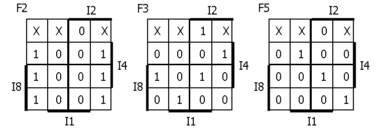
(a) Implement the three functions above
using the read-only memory (ROM) shown below. Place Xs where connections
need to be made in the OR plane. (5 points)
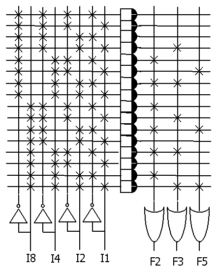
(b) Implement the three functions above using the programmable array logic (PAL) shown below. Place Xs where connections need to be made in the AND plane. Note that all outputs must be a sum of no more than three product terms but that you have the ability to form a fourth output that can be fed back into the array as an input. NOTE: please write the product term that each AND gate implements inside the AND gate symbol. (10 points)
(c) Implement the three functions above
using the programmable logic array (PLA) shown below. Place Xs where connections
need to be made in the AND and OR planes. Note that there can be no more
than eight total product terms for all three functions. NOTE: please write
the product term that each AND gate implements inside the AND gate symbol.
(10 points)
3. Sequential Logic (15 points)
Determine the fastest possible clock
period (the time between consecutive clock edges) for the circuit shown
below. You can assume that the gate delay of the NAND and NOR gates
is 2, the XOR gate's is 3, the inverter's is 1, the setup and hold times
for the flip-flops are both 1, and the propagation time of the flip-flop
is 2. Explain how you derived your value.
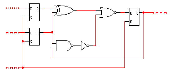
min clock period = FF prop time + comb. logic delay + setup time
min clock period = 2 + max(XOR + NOR, NAND + NOT + NOR) + 1
min clock period = 2 + max(3 + 2, 2 + 1 + 2) + 1
min clock period = 2 + max(5, 5) + 1
min clock period = 2 + 5 + 1
min clock period = 8Recall that the hold time of a flip-flop overlaps the propagation time.
4. Implementation of Sequential Logic (25 points)
(a) Derive a state diagram for an asynchronous
Mealy finite state machine that outputs a 1 whenever it sees the pattern
1110, 0111, 0110, or 1111 on its single input. Do NOT consider overlapping
patterns, instead look at each 4 bits as distinct. Use the skeletal
state diagram provided below and fill in the correct output value on each
arc. (2 points)
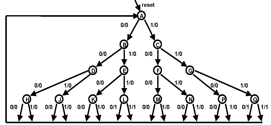
(b) Minimize the number of states in your state machine using the set-partition method discussed in lecture. List all equivalent states and draw a new state diagram (keep it in the same style as much as you can, 0 transition on the left, 1 transition on the right). (5 points)
(ABCDEFGHJKLMNPQ)
(ABCDEFGHJKMNP) (LQ)
(ABCDFHJKMNP) (EG) (LQ)
(ADFHJKMNP) (BC) (EG) (LQ)
(A) (DFHJKMNP) (BC) (EG) (LQ)
(A) (DF) (HJKMNP) (BC) (EG) (LQ)
(c) Derive a state table for your minimized
state machine. Keep it small by using don't cares. (3 points)
|
|
|
|
|
|
|
|
|
|
|
|
|
|
|
|
|
|
|
|
|
|
|
|
|
|
|
|
|
|
|
|
|
|
|
|
|
|
|
|
|
|
|
|
|
(d) Determine a minimum-width (smallest
possible number of bits) state assignment and explain how you came up with
your encoding. (4 points)
| state | code | reason |
| A | 000 | most common state, keeps number of 1s in truth table down |
| B | 001 | first bit has been seen |
| D | 010 | keep number of 1s down (like E, both from B) |
| E | 011 | second bit has been seen (like D, both from B) |
| H | 100 | keep number of 1s down |
| L | 111 | third bit has been seen |
(e) Write a pseudo-Verilog decription
(as close as possible to Verilog syntax but don't worry about being precise)
of your minimized state machine. Make sure to make your encoding
clear. (5 points)
module FSM (Input, Reset, Output)
input Input, Reset;
output Output;
reg Output;
reg present_state[2:0];
reg next_state[2:0];
'define A 3b'000;
'define B 3b'001;
'define D 3b'010;
'define E 3b'011;
'define H 3b'100;
'define L 3b'111;always @(posedge clk) begin
if (Reset) then present_state = 'A;
else present_state = next_state;
endalways @(Input or present_state) begin
Output = 0;
case (present_state)
'A: begin
next_state = 'B;
end
'B: begin
if (Input) next_state = 'E
else next_state = 'D;
end
'D: begin
next_state = 'H;
end
'E: begin
if (Input) next_state = 'L;
else next_stae = 'H;
end
'H: begin
next_state = 'A;
end
'L: begin
next_state = 'A;
Output = 1;
end
default: display("error");
endcase
end
endmodule
(f) Derive the logic to implement
the state machine. Do not bother drawing a circuit, simply write
down the Boolean equations for the output and each of the state bits.
The input is named In and the output is named Out. The state bits
should have names such as P1, P2, ... and N1, N2, ... for present and next
state, respectively. (6 points)
Encoded state table:
|
|
|
|
|
|
|
|
|
|
|
|
|
|
|
|
|
|
|
|
|
|
|
|
|
|
|
|
|
|
|
|
|
|
|
|
|
|
|
|
|
|
|
|
|
OUT = P1P2P3
N1 = P1P2
N2 = P1P2P3 + P1P2P3IN
N3 = P1P2P3 + P1P3IN
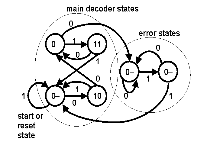
5. Finite State Machine Design (25 points)
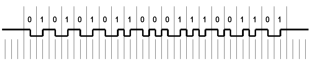
The Ethernet physical layer protocol encodes data using a method called Manchester encoding. In Manchester encoding, a "zero" is transmitted by first sending a 1 and then a 0, while a "one" is transmitted by sending a 0 and then a 1. When no packet is being sent, the line is kept at 1. Every packet starts with a 0 bit. The figure below provides an example of a packet containing the data 010101011000111001101. The tick marks below the waveform represent clock periods, those above represent "data periods" which correspond to two clock periods.
Derive a Moore state machine that decodes
an Ethernet packet. The input should be called E (for Ethernet) and
there should be two outputs, one for the data decoded (D for data) and
one for whether it is should be ignored or not (V for valid). Note
that when the line is quiet, consecutive bits will all be 1.
Therefore, you should make the decoder "reset" whenever there are a number
of consecutive 1s inconsistent with normal data transmission. Be
sure to handle the error condition of too many consecutive bits that are
0, as well. Your machine should keep V low and wait for two consecutive
1s to "reset".
This state diagram can then be reduced via state minimization to: