Lab # 3
DUE: In one week, at 1:30 pm
Collaboration Policy:
Unless otherwise noted, your group may collaborate with other CSE467
groups on the lab assignments. Collaboration means that you may discuss
the experiments and make notes during the discussion, but you may not copy
another groups work when doing the experiments; you may not copy experimental
results from another group; and you may not copy any part of another groups
lab report. In addition, every individual in a group must understand the
experiments, must participate in the writeup, and should understand the
results. Collaboration does not mean that one person may perform the experiments
and another write up the resultsall lab partners must share equally in
all parts of the lab assignment.
Late Policy:
The lab assignments are due in one week, at the beginning of your lab
section. Assignments handed in after lab will incur a 10% penalty; the
penalty will increase by 10% for each additional day late.
Overview:
The purpose of this lab is to give you experience using a logic analyzer.
The lab:
Answer all the questions in this handout in your lab writeup. Show
all of your work, and remember, your solutions must be legible.
The points for each problem are noted on the problem statement.
Parts you will need:
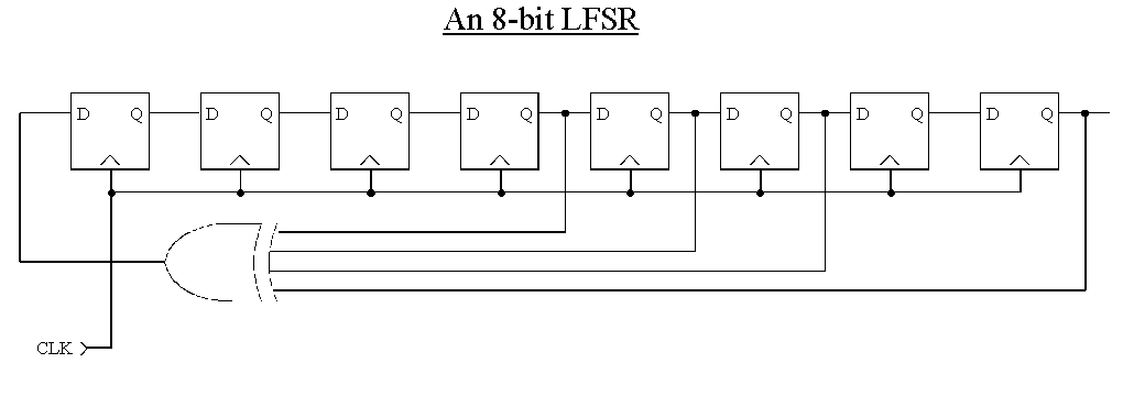
Assemble the LFSR shown below. Use an SN74LS299 universal shift register and a SN74LS86 quad 2-input XOR. Connect feedback into the first D flip-flop as shown. You will need to construct the 4-input XOR from 2-input XORs. Connect power, ground, and clock. Put decoupling across the IC power and ground leads. Run the clock at 1MHz. Remember to put a 4.7k resistor from the clock-source output to Vdd.
Attach logic analyzer probes to the outputs of each of the 8 flip-flops.
Acquire the 8-bit data, and display them as (a) a list, and (b) a waveform.
You may need to jump-start the LFSR out of the 00000000 state by touching
the input to Vdd. You may use any triggering method you choose
(manual or stop-on-pattern). Print the data in list and waveform formats
(print postscript to file, transfer to a floppy, and then dump to a printer
later). Hand in the list and waveform pictures with your writeup. Also
document the analyzer settings that you used (i.e. clock rate, internal
or external clock, trigger method, etc.). You may print these settings,
or just write them down.
Assemble a 16-bit LFSR using 2 SN74LS299 universal shift registers in
series. Use a 4-input XOR for the feedback. The inputs to the XOR must
come from flip-flops 11, 12, 13, and 16. Attach 16 logic analyzer probes
to the 16 flip-flop outputs, and acquire the 16-bit data. Trigger on the
pattern 0011001111110000, and print a listing of the 16-bit patterns that
occur after 0011001111110000 (show at least 4 patterns in the list). Document
the analyzer settings that you used (i.e. clock rate, internal or external
clock, trigger method, etc.). You may print these settings, or just write
them down.