 Once you have the circuit connected, test it to make sure that it works.
 CSE 467: Advanced Digital Design
(Winter 2000)Lab 4 - Introduction to the XS40 Board
This lab is due one week from today. There are six parts to this lab. You may not be able to finish all six parts during lab, but you will have until the next lab session to complete everything.
Collaboration Policy:
Unless otherwise noted, your group may collaborate with other CSE467 groups on the lab assignments. Collaboration means that you may discuss the experiments and make notes during the discussion, but you may not copy another group’s work when doing the experiments; you may not copy experimental results from another group; and you may not copy any part of another group’s lab report. In addition, every individual in a group must understand the experiments, must participate in the writeup, and should understand the results. Collaboration does not mean that one person may perform the experiments and another write up the results—all lab partners must share equally in all parts of the lab assignment.
Late Policy:
The lab assignments are due in one week, at the beginning of your lab section. Assignments handed in after lab will incur a 10% penalty; the penalty will increase by 10% for each additional day late.
In this lab will you will learn the following:
This lab has one handout:
Part 1 - Compile the FIFO design
In this part, you will compile the Xilinx FIFO design so that it can be loaded into an FPGA. The
\\ifilesrv1\cse467\Winter00\ folder contains the Xilinx project Lab4 that has the FIFO design you have already worked on. In addition, it has a top-level schematic that instantiates the FIFO and connects it to the pins of the FPGA. Note that each input signal is connected to an IPAD and IBUF symbol, and each output signal is connected to an OPAD and OBUF symbol. These represent the circuit that connect the signals in the FPGA to the pins. The pin number is specified using the LOC paramber on the PAD symbol - you can enter and change this by double-clicking on the PAD. (Later on we will learn a different way to do this.) Besides the FIFO connections, this top-level schematic disables the microcontroller and SRAM by connecting a number of their pins to Vdd and GND. Make sure you understand this top-level schematic.The Foundation tools will compile your design when you click on the Implementation button in the Project Manager window. The result of this process (unless there are errors) is a "bit file". This is an object file that can be downloaded to the FPGA. After you have performed the implementation, you should take a look at the reports that Foundation generates. These can be found by clicking the Reports tab in the Project Manager. Pay particular attention at this point to the first three reports. We will learn a lot more about what happens during implementation, but for now we can treat it as a black box. By the way, we recommend that you not use the versioning feature of the tools. In fact, it is a good idea to delete the implementation data (in the Project Menu).
Note: The Verilog compiler (called FPGA Express) has already been run whenever you edited the Verilog file and you would have fixed any errors then.
The XS40 board contains a Xilinx 4010XL FPGA along with a microcontroller (which we will not be using) and a 32Kx8 SRAM (which we will use later). The schematic in the XS40 documentation shows how these three components are connected together. At this point, you do not have to understand these connections. We have already assigned the pins of the FPGA for you in the top-level schematic. (You might be interested which pins we chose.)
Note: Before you start using the XS40 board, you might want to test it to make sure it works OK. Plug the small power supply into the XS40 board and the PC parallel port cable into the connector on the XS40 board. In a DOS window, run the command:
xstest xs40-010xl
This will test the board by programming the FPGA which will then run a test. The 7-segment display will go through some paces and eventually end up with ‘O’ for OK, or ‘E’ for error.
The key thing about the XS40 board is that the pins of the board around the periphery are each connected to the Xilinx chip pins with the same numbers. That is, you can connect to a Xilinx chip pin by just connecting to the protoboard connection for the board pin with that number. Be careful figuring out the numbers though!
The most important connection for the XS40 board is the GND connection - pin 52. You must connect pin 52 to the prototyping board GND. Failure to do so can result in a blown Xilinx chip ($40).
We will give you a chip (a 24-pin PLD) that will provide the test data for the FIFO implemented in the FPGA. To run this chip, first turn on Reset, then turn it off. The chip will generate random data to the FIFO as well as random Reads and Writes.
The pins of this chip are numbered from pin 1 to 24 around the chip in the usual way. Here are the pinouts of the test PLD:
Pin 1 - CLK (same clock as Xilinx chip CLK)
Pin 2 - Reset (same reset as Xilinx chip reset)
Pins 21-14 - DataIn[7:0] Input data to the FIFO
Pin 22 - Write signal for the FIFO
Pin 23 - Read signal for the FIFO
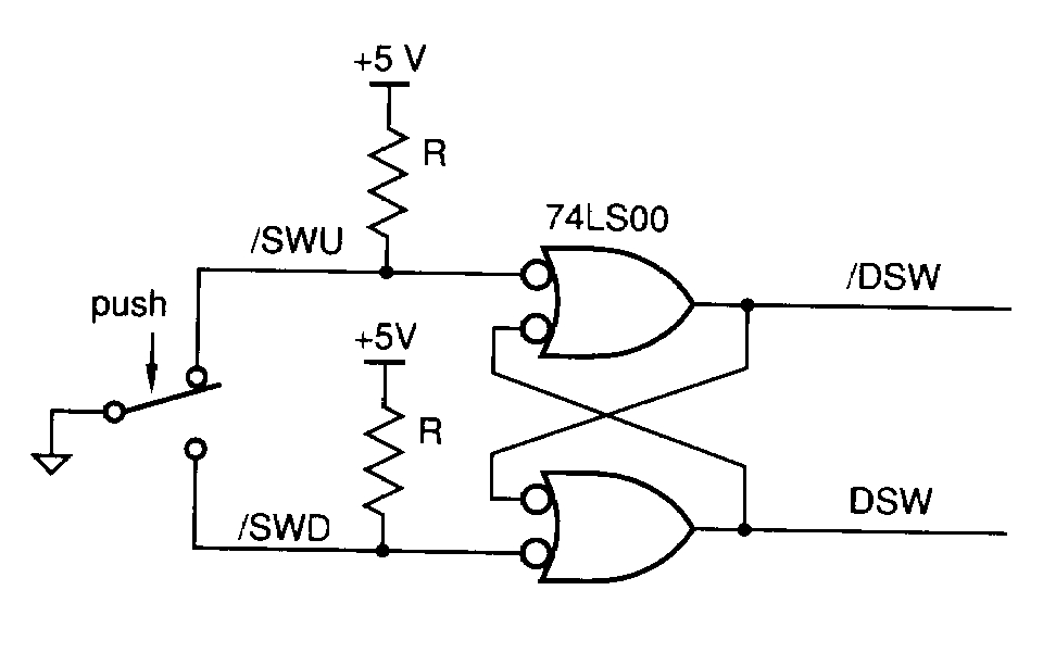
You could provide the reset input by a simple wire that you connect to Vdd or GND. However, it is a lot better to use a switch, which you should have in your DesignKit. A switch is made using contacts that are connected or disconnected. The problem with switches is that when the contacts are connected, they bounce, which means you get multiple edges instead of one clean edge. We will fix this problem with a simple circuit and a 3-terminal push-button switch.
Find a pushbutton switch in your Design Kit that has three terminals. One of these terminals is a "common" terminal while the other two are "normally-closed" (NC) and "normally-open" (NO). When the switch is not being pushed, it is in the open state. In this state, the common terminal is connected to the NC terminal. When the switch is being pushed, the common terminal is connected to the NO terminal. Use the multimeter to determine which terminal is which by measuring the resistance between terminals. (We’ll show you how to use a multimeter if you haven’t used one.)
We can debounce a switch by using a latch and using both the normally-open and normally-closed terminals of the switch as shown in the figure below. The first contact of the switch will cause the latch to change state. Then, even if the switch bounces, the latch will stay in the same state. Use a 74LS00 chip to implement the switch debounce circuit.
Once you have the circuit connected, test it to make sure that it works.
Part 4 -- Connect up the Logic Analyzer
Before you run the circuit, you will need to connect up the logic analyzer so that you can see whether the FIFO is working properly. You will need to sample all the FIFO interface signals: DataIn[7:0], DataOut[7:0], Read, Write, Empty and Full and this will take 3 sets of 8 wire leads and two cable headers. Connect your wire leads so that it will be easy to unplug them from the logic analyzer and then plug them in again later. You can keep the wire leads plugged into the board until you are finished with them.
You are now ready to try out your circuit by downloading the Bit File (FIFO.bit) for your design. Before you do this you must connect power to both the protoboard and the XS40 board, and connect the PC parallel port cable to the XS40 board.
IMPORTANT: Before you plug power into the XESS board, doublecheck to make sure that you have the GND signals connected correctly. Use the multimeter to measure the resistance between the grounds on the two boards. It should be 0. Also measure the resistance between Vdd and GND on the two boards - it should be very high (e.g. high enough not to register).
After you have setup the data signals, set up the trigger to trigger on the reset signal going low. Now capture the data when you press and release the reset button. Look at the signals and determine whether the FIFO is behaving correctly. Print out one (or more) windows that show all the following cases: