CSE467: Advanced Logic Design
Carl Ebeling, Winter 1999
Homework 2
Distributed: Jan. 20 - Due Friday, Jan. 29 (beginning of class)
Problems:
-
Katz 6.21
-
Katz 6.22
-
Design a circuit that implements a 3-bit gray-code counter that counts
0, 2, 6, 4, 5, 7, 3, 1. That is, do the necessary synthesis and draw a
schematic with the resulting combinational logic and registers.
-
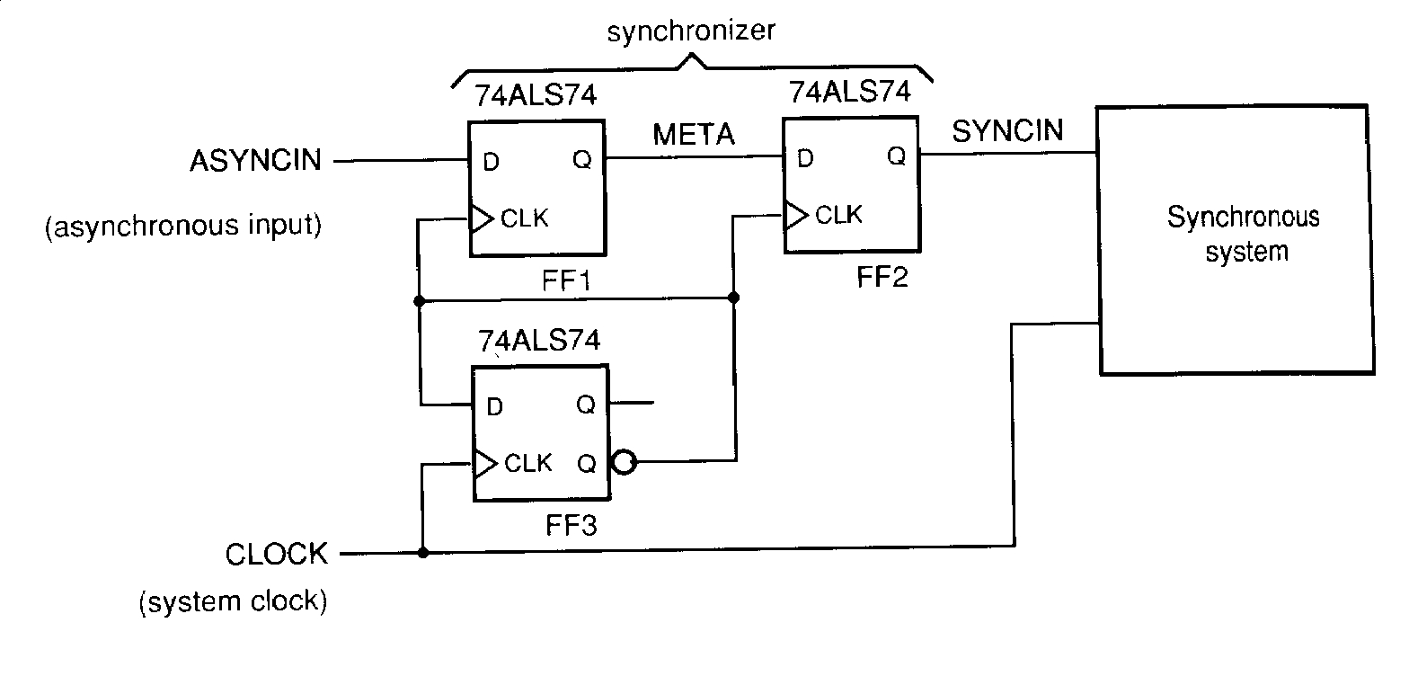
Calculate the MTBF of the synchronizer shown in the figure below, assuming
a clock frequency of 25 MHz and an asynchronous transistion rate of 1 MHz.
Assume that the setup time and propagation delay for the 74ALS74 are both
10 ns.
-
Design an 8-bit shift register with synchronous control inputs LD, ShL,
and ShR. LD causes the shift register to load from its inputs. ShL causes
it to shift its contents left and ShR shifts the contents right. Use the
Xilinx schematics editor to design this shift register using gates, multiplexors
and registers from the Xilinx library. Write a simulation script to simulate
this shift register.

ebeling@cs.washington.edu