CSE467: Advanced Logic Design
Carl Ebeling, Winter 1999
Lab 3
Sequential Circuits with Verilog and FPGAs
Distributed: Jan. 25
Simulation: Feb. 5
Completed circuit due: Feb. 12
Objectives
After completing this lab you will know how to:
-
Use Verilog to specify finite state machines
-
Include Verilog components in your schematics
-
Synthesize the Verilog components
-
Simulate and debug sequential circuits
From now on, you will be working in teams of two. However, each person
will also have to design their own personal FSM to write their name on
the LCD display.
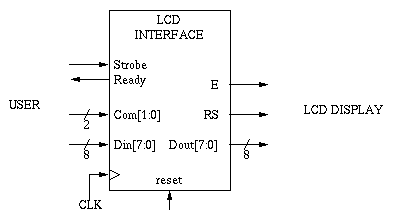
I. Design Problem: LCD Interface
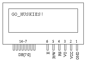
In each DesignKit there is an LCD display which can display two lines of
16 characters.
This LCD display is operated through a set of control and data lines as
described in detail in the next section. Your first job is to design a
simple interface, as shown in the next figure, to this display which you
can use for the remainder of the course. The user will control your interface
using two signals, Strobe and Ready, a set of Command signals and a set
of Data signals. The Strobe line is an input which tells your circuit to
display a new character. When Strobe goes from low to high, your circuit
should read the character on the data lines and display it on the LCD display.
The Ready line is an output that tells the user when your interface is
ready to accept another character. The user looks at Ready and waits until
it is asserted before asserting Strobe. Your interface will immediately
deassert Ready until it has finished displaying the character. Strobe and
Ready form a handshake protocol that is very common in interfaces.
The User waits for Ready to be asserted, then asserts Strobe. The
User then waits for Ready to be deasserted by the interface, which indicates
that the interface has seen the Strobe signal, before deasserted Strobe.
The User then waits for Ready to be asserted before starting a new transaction.
This is called an asynchronous protocol because no assumption is made about
how slow or fast the interface is.
The command is encoded in two bits as follows:
00 - Write a character to the screen
01 - Clear the screen
10 - Backspace
11 - Home
Your interface samples these command signals when Strobe is asserted and
performs the appropriate actions based on the command. If the command is
to write a character to the screen, then the 8 Data lines contain the character
to be written. Note that if you never want to use Backspace or Home, the
high order bit of the Command can be tied to 0.
Testing Your LCD Interface
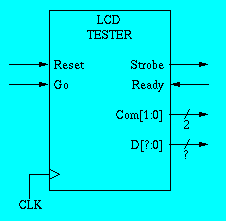
You should start out with a simple FSM test circuit that executes the commands
you want to test. This test circuit should have a reset and go input.
When the go signal is asserted (using a switch), the test circuit should
execute a few LCD display commands and then quit. Each team member
should then write an FSM circuit that displays their name to the LCD display.
You can get fancy if you want, for a bit of extra credit. See the
LCD documentation for details.
The LCD Screen
Your interface circuit is responsible for converting a very simple interface
protocol to a somewhat more complicated protocol used by the LCD driver
interface. This interface takes instructions or data depending on the value
of the RS wire. The table below shows the instructions you will be using.
Four instructions are required to initialize the display for the configuration
we require (a 1 line by 16 character display). These are shown in the first
four lines of the table. So your control logic must be sure to issue these
instructions whenever it is reset.
Operation       RS      R/W     DB7...DB0
Clear Display   0       0       0000 0001
Function Set    0       0       0011 00**
Display ON      0       0       0000 1100
Entry Mode Set  0       0       0000 0110
Write Character 1       0       DDDD DDDD
Backspace       0       0       0001 00**
Return Home     0       0       0000 001*
Read Character  1       1       DDDD DDDD
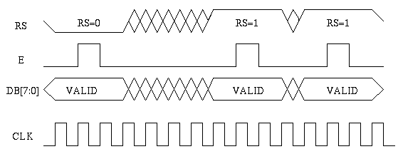
The timing constraints that must be satisfied when writing information
into the display are a little complicated. Basically, the display samples
the RS line on the rising edge of the enable signal (E) and the DB lines
on the falling edge of E. To keep things simple, the set up and hold time
for RS should be one cycle before and after the rising edge of E, respectively.
Similarly for the DB lines and the falling edge of E. The only other timing
information of importance is to allow 1.6ms for the display to actually
clear (the internal controllers takes some time to actually go and enter
0s in the internal memory of the display unit).
Since your never needs to perform read operations, the R/W control line
can be tied directly to GND. For normal character write operations, the
RS signal should be 1. To execute a command, the RS signal should be 0.
The easiest way to perform a write is by asserting the enable signal (E)
for one clock cycle during which RS and data are both stable. So the signals
generated by your interface would look like:
You must ensure that the number code is stable while this is happening.
(This will not be a problem, because you can tell the user that you are
busy while you are doing this.) However, you should ensure that RS is stable
for a cycle before and after the write operation is performed. You will
need to do this in your controller's finite state machine. Since the Enable
signal is used to clock data into the display, it should be hazard-free
(no spurious glitches). The easiest way to ensure this is to make it a
direct output of a flip-flop.
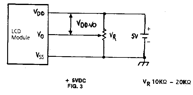
In addition to connecting Vdd (+5V) and GND to the LCD display, you
will need to connect the VO input through a variable resistor to provide
a voltage between 0 and +5. This input governs the contrast of the
display. We will give you the variable resistor - you will have to
use the ohmeter to figure out the terminals and how it works. The
figure below (copied from the LCD documentation) shows how the connections
should be made.
Details, Details, Details...
Part of designing a circuit to solve a problem is defining what the problem
is. Most problem descriptions are hazy, incomplete and ambiguous. One of
the tasks when designing is to turn such a description into a precise specification.
Before you begin to design, ask yourself what is missing and write down
as precise a specification as you can. Hand in this written specification
along with your circuit design.
NOTES:
-
Don't forget to provide a reset input to both parts of your circuit.
-
The XESS board runs at 12MHz, which is way too fast for the LCD display.
The data sheet indicates that it takes 40 microseconds to execute a command
(except for HOME and CLEAR which take 1.6 milliseconds). We could
use counters to count off the almost 400 cycles we would have to wait between
commands. Instead we will divide down the clock so that it runs at
100KHz. instead of 12MHz. Do this by using a 7-bit counter and connecting
the internal clock to the high-order bit of this counter. Put the
BUFG on this counter output so that the internal clock signal is buffered.
For the HOME and CLEAR commands, you will have to wait for 1.6msec. before
asserting the READY signal, so you will have to do some counting.
Entering and Simulating your Design
Divide each design into reasonably-sized components, such as registers
and counters and combinational logic. Draw a top-level schematic for your
design, including the components that you need. (Work with your TA if you
are not sure how to define this hierarchy.) You can use Verilog to
specify both your sequential (e.g. FSMs) and combinational (e.g. code converter)
components. You can also use library and LogiBlox components.
You should simulate your circuit as best you can, and then download
it into the XESS board. Use XESS board pins 8 and 9 for input switches
(reset and go) and pins 18, 19, 20, 23, 24, 25, 26, 27, 28, 29, 30 to connect
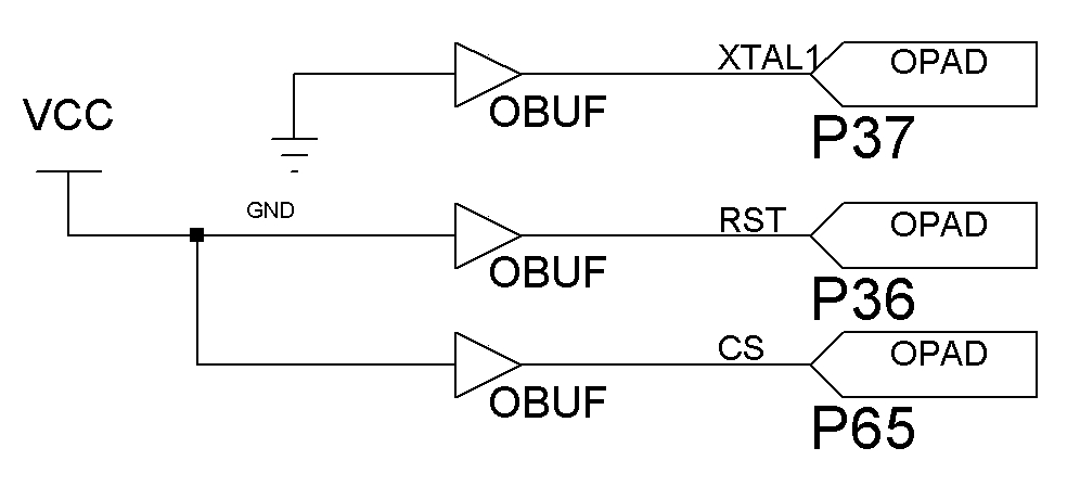
to the LCD display. In addition, include the following connections
in your top-level schematic. This will disable the microcontroller
on the XESS board so that it doesn't get in the way.
Please be very careful with the boards - handle them carefully and make
sure that the GNDs are connected between the protoboard and the XESS board.
Since you will be sharing the boards at least for a little while, make
sure that you can disconnect and reconnect it to your protoboard quickly
and reliably. What I do is put little tags on the interface wires
that indicate how they are connected.
Schedule:
Turn in by Feb. 5:
-
Design documentation: Whatever notes that we need to understand your design.
Remember, you are responsible for making sure we understand your design.
If we can't understand it, we can't grade it.
-
Printout of all schematics
-
Printout of all Verilog modules
-
Printout of simulation script, log file and waveform
-
Signature of TA
Turn in by Feb. 12:
-
Completed and working circuit
-
Signature of the TA to show that you demoed the circuit and that
it is working correctly.
Don't procrastinate! Getting the LCD circuit to work properly can
be tricky. Moreover, in next week's lab you will be learning how
to use the logic analyzer. You will be able to use the logic analyzer
to debug your circuit, but you won't be able to spend the whole lab time
working on this circuit.
ebeling@cs.washington.edu