CSE370 Final Exam (
Please read through the entire examination first! This exam was designed
to be completed in 100 minutes (one hour and 40 minutes) and, hopefully, this
estimate will be reasonable. There are 4 problems for a total of 100
points. The point value of each problem is indicated in the table below.
Each problem and sub-problem is on a separate sheet of paper. Write your answer neatly in the space provided. If you need more space (you shouldn't), you can write on the back of the sheet where the question is posed, but please make sure that you indicate clearly the problem to which the comments apply. Do NOT use any other paper to hand in your answers.
The exam is CLOSED book and CLOSED notes. Please do not ask or provide anything to anyone else in the class during the exam. Make sure to ask clarification questions early so that both you and the others may benefit as much as possible from the answers.
Good luck and have a great winter break.
Name: Jill Engineer
ID#: 050370
|
Problem |
Max Score |
Score |
|
1 |
15 |
15 |
|
2 |
20 |
20 |
|
3 |
35 |
35 |
|
4 |
30 |
30 |
|
TOTAL |
100 |
100 |
1. Boolean Algebra (15 points)
(a – 5 pts) The following circuit implements
a Boolean function of 5 variables (A, B, C, S1, and S2). It uses five 4:1 multiplexers. Note that S1 and S2 are simply used to
select one of four functions of A, B, and C. Write the equations for these four functions. We’ll call them F0, F1, F2, and
F3. Inputs to the multiplexer are
numbered from 0 to 3 top to bottom, control inputs are high-order on the left,
low-order on the right.
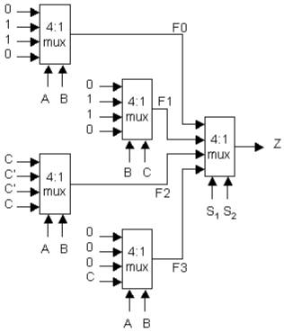
F0 = A xor B = A’B + AB’
F1 = B xor C = B’C + BC’
F2 = A xor B xor C = A’B’C + A’BC’ + AB’C’ + ABC
F3 = ABC
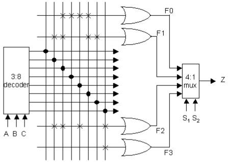
(b – 5 pts) We will now use a new kind of
programmable logic called a DAL (Decoder Array Logic) to re-implement our logic
function. The schematic of a very
useful DAL370V4 component is given below.
Show which connections need to be made to the OR gates to implement Z
(show the connections as an X at the intersection of the OR input line and the
decoder outputs). Decoder outputs
are numbered 0 to 7 from top to bottom, control inputs are high-order on the
left, low-order on the right.
(c – 5 pts) On the other hand, it might be
more efficient to implement this function in a
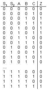
2. Sequential Logic (20 points)
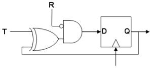
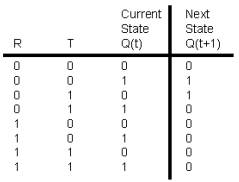
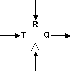
(a – 5pts) You are given a basic edge-triggered D-type flip-flop. Your task is to turn it into a new kind of flip-flop that we’ll call a toggle (or T-type) flip-flop. It will have two inputs in addition to the clock signal: R, a synchronous reset signal; and T, the toggle input. When T is high at a positive clock edge, the value of Q will become the opposite of what it was previously. When T is low at a positive clock edge, the value of Q will not change. Using only simple gates (OR, AND, NOT, XOR – with as many inputs as you need) around the D-FF, create a T-FF. Fill in the equation for D as well as drawing a circuit around the D-FF below left. Your objective is to create a module like the T-FF symbol below right.
D = f(R,
T, Q) = R’T’Q + R’TQ’ = R’(T xor Q)
this truth-table makes the synchronous
reset dominant over T.

(b – 10 pts) By now, you have your T-FF ready to go. Design a reset-able 4-bit binary up-counter with enable using your new T-FF as the replicated component. Four of them are provided below. Draw your logic around them. Again, you should only need to use simple gates (with any number of inputs). Clearly label: the reset (RESET) signal for the entire counter; 4 output bits (labeled with LSB – least-significant bit – and MSB – most-significant bit – from left to right); and the counter’s enable (ENABLE) signal. When enable is low, the counter should not change value. When ENABLE is high, it should count to the next binary value.
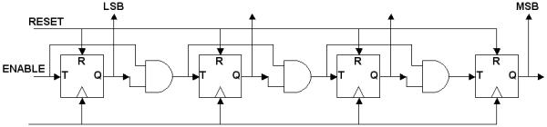
In a binary counter, the low-order toggles at every count. Thus, ENABLE is connected to the T
input of the LSB. The second
low-order bit toggles when the counter is ENABLEd and the previous bit is 1. Similarly for each subsequent bit,
however, this would require a larger and larger AND gate at each stage. We can use just a two-input AND at each
state if we daisy-chain the toggle inputs. The second bit toggles if the previous bit is 1 and is also
enabled to toggle. And, so on.
(c – 5 pts) Do you foresee any issues with
making this type of counter into a longer counter (say, 32 bits long)? Write a couple of sentences at most.
If you made a daisy-chain of 2-input AND gates, then the issue is that
this chain grows linearly with the size of the counter.
If you used an AND gate with inputs from all previous stages, then the
issue is that the fanin of this gate grows linearly with the size of the
counter.
In either case, the delay will get prohibitively long.
3.
For this problem, you will implement a
finite-state machine using the parts provided below. However, you’ll have to figure out what the parts can do for
you by reading their Verilog models.
Read these Verilog descriptions carefully.
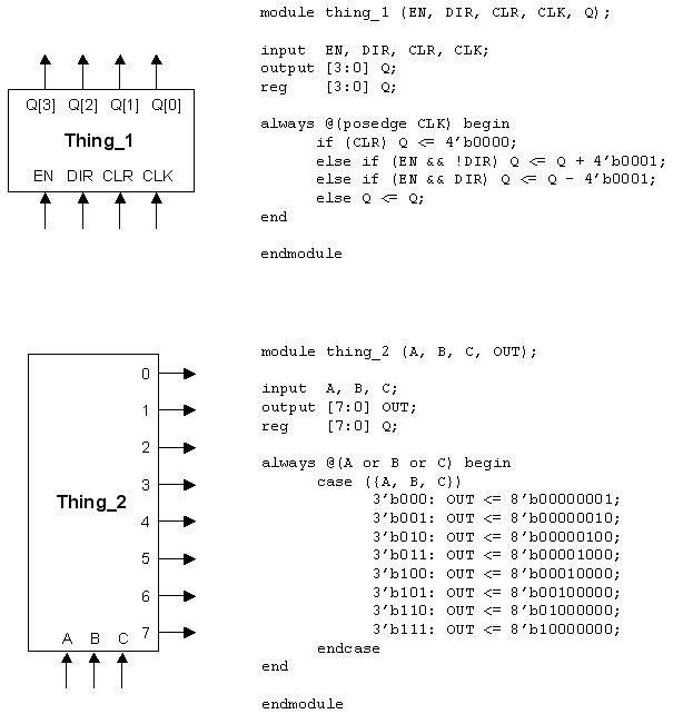
(a – 10 pts) What are the two components you’ve been provided? Describe the functions implemented by Thing_1 and Thing_2 with at most a couple of sentences for each. Be specific, complete, and relate them to parts you already know.
Thing_1 is a ….
4-bit binary up/down-counter with count enable, direction input, and
clear.
Thing_2 is a ….
3-8 decoder with A being the most-significant and
C being the least-significant control bits.
(b – 10pts) In one of the lab assignments this quarter, you
implemented a finite-state machine to play a simple “tug-of-war” game using two
push buttons and seven LEDs. The
state diagram for that FSM is given below. You can assume you have the two inputs, L and R, they are
high for exactly one cycle whenever the left and right push buttons are
pressed. 
For
this problem, you will re-implement the state machine using the parts provided
in part (a). Begin by completing
the symbolic state table below.
You will need to use Thing_1 to realize your state. First, choose an encoding for state S1
through S6 that will be compatible with using Thing_1, then complete the state
table below (using symbolic states).
Start by entering the next state for each possible state transition. Then, fill in the values for EN and DIR
that you will need to make that state change occur in Thing_1 (make sure to use
don’t cares). RESET will be
connected to the CLR input of Thing_1.
(c – 5 pts) Derive equations for EN and DIR from the table in part (c). You do NOT need to use K-maps, in fact, it is NOT recommended you do so as they have high dimensionality. Instead, exploit the don’t cares to come up with the simplest functions you can of L, R, and the current state of Thing_1 (Q3, Q2, Q1, and Q0).
EN = (L xor R) (S0’) (S6’) = (L xor R) (Q4’
Q2 Q1)’ (Q4’ Q2 Q1)’
(we don’t need to use Q8 due to
all the unused state codes that act as don’t care)
DIR = L
(again, taking advantage of the many don’t cares)
(d – 10 pts) Now, it is time to wrap up our tug-of-war game. Show, how you would wire up the
components provided below: Thing_1, Thing_2, and the bank of seven LEDs. Use whatever simple gates you need to realize
the functions for EN and DIR you derived in part (c). Clearly label the L, R, RESET, and CLK inputs to your
completed circuit. You should only
need wires to connect to the inputs and outputs of Thing_2 and the LEDs.
The logic for EN and DIR is given in the previous part. Their equations use L, R, Q4, Q2, and
Q1 as inputs. RESET is simply
connected to CLR of the counter.
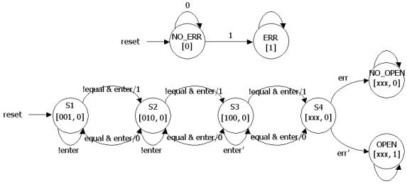
4.
The state diagram below is the one we used in lecture to describe a 3-value-key combinational lock.
However,
the program code we used did not correspond to this state diagram exactly. A more accurate rendition is the state
diagram shown below. Note that it
consists of two parallel finite state machines that communicate through two
signals (set_err and err). The
machine with two states is a
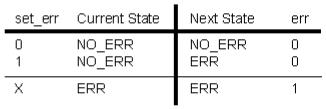
(a – 5 pts) Below are two symbolic state tables. The one for the 6-state FSM needs to be completed. The one for the 2-state FSM is already completed. Complete the first state table – use symbolic states.
Symbolic state table for the 6-state FSM:
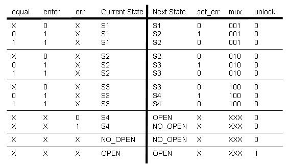
Symbolic state table for the 2-state FSM:
(b – 10 pts) Select a state encoding for the two state machines:
ERR
= 1
NO_ERR
= 0
S1
= 0 001
S2 = 0 010
S3
= 0 100
S4 = 0 000
OPEN = 1 000
NO_OPEN = 0 111
Explain
in a few sentences why you chose the state encoding above.
For the 2-state FSM, it is easy to use a single bit to distinguish the two
states and make its value the same as the single Moore output (err).
For
the 6-state FSM, it is good to use the mux control outputs (mux) for three of
the state bits. They provide a
on-hot code to distinguish S1, S2, and S3. The unlock output can be used to distinguish the OPEN state
and must be 0 for all the others.
Given these 4 state bits (unlock = state[3] and mux = state[2:0]), we
still need to choose the assignment of the mux outputs for OPEN, NO_OPEN and
S4. We choose 000 for S4 and OPEN
and 111 for NO_OPEN. This
assignment has a smaller number of 1s and is symmetric for all the state bits
thus leading to similar equations.
(c – 5 pts) Complete the Verilog description for the 2-state FSM provided below:
module FSM_2 (clk, reset,
set_err, err);
input clk, reset, set_err;
output err;
reg [ _0_ : _0_
] state;
parameter ERR = ___1__
;
parameter NO_ERR = ___0__
;
always @(posedge clk) begin
if (reset) state <=
NO_ERR;
else if (set_err) state
<= ERR;
else state <= NO_ERR; //
this line not required
end
endmodule
(NOTE:
It is technically correct to replace that line:
if (set_err) state <= ERR;
with
state <= set_err;
However,
although this change would make the description shorter, it would tie the
Verilog code to the state assignment we chose. This is generally not a good
policy. Let’s leave it to the
optimization tool to figure it out given our code and state assignments.)
(d – 5 pts) Complete the Verilog description for the 6-state FSM provided below:
module FSM_6 (clk, reset,
equal, enter, err, set_err, mux, unlock);
input clk, reset, equal, enter, err;
output set_err, unlock;
output [2:0] mux;
reg [ _3_ : _0_
] state;
parameter S1 = _0001_
;
parameter S2 = _0010_
;
parameter S3 = _0100_
;
parameter S4 = _0000_
;
parameter OPEN = _1000_
;
parameter NO_OPEN = _0111_
;
assign unlock = state[3];
assign mux[2:0] =
state[2:0];
always @(posedge clk) begin
case (state)
S1:
if (enter) state <= S2; else state <= S1;
S2:
if (enter) state <= S3; else state <= S2;
S3:
if (enter) state <= S4; else state <= S3;
S4:
if (err) state <=
NO_OPEN; else state <= OPEN;
OPEN: state <= OPEN; //
not required
NO_OPEN:
state <= NO_OPEN; //
not required
default:
$display(“invalid state reached”);
endcase
end
always @(state or equal or
enter) begin
set_err = 0;
if ( ((state == S1) ||
(state == S2) || (state == S3))
&& enter && !equal) set_err = 1;
end
endmodule
(e – 5 pts) Why was the set_err output of the 6-state FSM made to be an asynchronous Mealy output? Would our combinational lock still function properly if this FSM were realized as a synchronous Mealy machine?
set_err has to be an asynchronous
Mealy output because we need the 2-state FSM to react quickly and go to the ERR
state and assert its output, err. If set_err had to wait until a clock edge to be set, then
the FSM could enter S4 at the same time the other machine enters ERR and not
see the err output being
set to 1. This would lead to the lock
opening even though the last input value entered was wrong.