CSE370 Laboratory Assignment 5
Edge-Triggered Flip-Flops
Distributed: 3 November 2003
Due: 7 November 2003
Objectives
In this laboratory assignment you get to know edge-triggered D-type
flip-flops. You will be using the '74 component in your kit (see map). This will be the first time you
use a clock signal and learn about both synchronous and asynchronous
inputs to the flip-flop. D-type flip-flops are the primary
sequential logic device and we will be using them throughout the
remainder of the quarter.
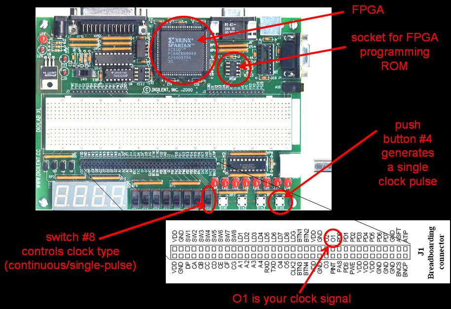
XLA5 Prototyping Board
To do this laboratory assignment, as well as all the future ones, you
will need a periodic clock signal. We have programmed the large
FPGA on the XLA5 board to provide you a convenient clock that will make
it easier for you to debug your circuits. The figure below shows
the FPGA as well as the socket that will hold the programming ROM for
the FPGA. The programming ROM holds the configuration file for
the FPGA - the collection of 0s and 1s that will configure the FPGA to
have the functionality we desire. This program was derived using
the Aldec tools.
Here is the basic idea for the clock generated we've constructed for
you. Rather than having you deal exclusively with a
crystal-generated clock signal that runs continuously, we've programmed
the FPGA to deliver a more versatile clock signal. Using switch
#8, you can set the clock into one of two modes (LED #8, the right-most
LED follows the value of this switch). In the first
mode, with the switch set to 1 and LED #8 on, the clock runs
continously with a nice slow
frequency of 1.537KHz (or a period of 650 microseconds). In the
second mode, with the switch set to 0 and LED #8 off,
there is a single clock pulse whenever push button #4 is pressed.
This mode allows you to single-step your
sequential circuit. The width of the clock pulse is the same as
when the clock is running continuously (nominally, high for half a
period or 325 microseconds). This clock was chosen to be slow
enough that we would not have to be concerned with the delay of the
logic during the laboratory assignments.
Once you are done
debugging, you can flip the switch into continuous clock mode.
The figure below provides the details.
Tasks
- The '74 has 2 D flip-flops in one package (see map).
You'll note each flip-flop has a data input, D, a clock input, CP, two
outputs, Q and Q', and two additional inputs, SD and CD. These
last two are active-low (they have an affect when 0 and none when 1)
asynchronous set and clear inputs. Insert the '74 chip into your
protoboard and connect the D input to one of the switches, the clock
input to O1, and Q to one of the LEDs. Make sure to also connect
SD and CD to a logic 1 (VDD will do).
- Spend some time experimenting with the flip-flop. Set the
clock switch to pulse mode. Set the D input to a value, push
button #4 to generate a clock pulse. What happens to the LED you
connected to Q? Try a different value of D and push the button
again. Try changing D back and forth while not pushing button
#4. Note how Q only changes after you press the push
button. This is a synchronous flip-flop, changes in the output
only occur after a rising clock edge (positive edge-triggered).
Now repeat this in continuous clock mode. What is the difference?
- Now it is time to experiment with the asynchronous set and clear
inputs. Connect these to switches instead of the logic 1 they
were previously connected to. Make sure the switches are
initially set to output a 1. Now, set the value of Q to 0 using
the D input and the push-button. Flip the SD switch. What
happens? Did you have to press the push-button?
Asynchronous input take affect immediately, without waiting for the
next clock edge. Repeat the experiment with CD instead of
SD. Try setting both SD and CD to 0 (set and clear at the same
time), which dominates? Does the flip-flop set or clear?
- The last task is to create a simple two-bit shift register.
Wire up the second flip-flop and set its D input to be the Q output of
the first flip-flop. Connect two LED to the Q outputs of the two
flip-flops. Set the D input of the first flip-flop to 0 and push
button #4 a couple of times. Make sure you've connected all the
CD and SD inputs to logic 1 (failure to do this will cause your
flip-flops not to work as expected as an unconnected pin may be
interpreted as a 0 causing the flip-flop to set or clear). Now,
set the D input to 1 and push button #4 once, then again. What do
you observe on the LEDs? Convince yourself that the circuit is
functioning as a 2-bit shift register and demonstrate this to the TAs
to be checked off for the assignment..
Comments to: cse370-webmaster@cs.washington.edu (Last Update:
)