Lab 1&2: An Introduction to SystemVerilog and Digital Components
Overview
The first lab will introduce you to the Altera’s Terasic DE1-SoC development board and our primary design tool this quarter, Intel's Quartus Prime. Both of these components are very important for all future labs so please pay attention.
Be sure to read the before getting started so you know how to format your answers as you go.
Instructions
Task 1 – SystemVerilog Design and Simulation
The designs in this class will be done through the Intel Quartus Prime software. This is preloaded on machines in the lab (CSE 003), and you are free to do all the work on these PCs. However, you can install the software on your own computer, if desired, by following the page.
Open the and complete Sections 0 through 8. You will simulate two designs: mux2_1 and mux4_1. Be sure to do all of the steps and ask the course staff for help when you encounter issues. During your lab demo, you will need to show your simulation of mux4_1 and give a brief verbal explanation of what mux4_1 actually does.
Task 2 – Logic Investigation
Read through the document. Make sure you know where the LEDs, switches, and push buttons are on the DE1 and then connect it to your computer and power on your board. Feel free to play around with preloaded program to get a feel for the board inputs and outputs.
Now finish the rest of the Quartus Tutorial to program your board with the provided top-level module lab1.sv (code). Refer to the code comments and play with the appropriate inputs to discern the logical behaviors of our input and output signals:
- Which logical value (0 = FALSE = GND, 1 = TRUE = VDD) turns the red LEDs on?
- Which position (up or down) of the slider switch outputs a TRUE?
- Which position of the push button (pressed or unpressed) outputs a TRUE?
Task 3 – Add Simple Logic
Now modify lab1.sv to implement the following additional logic. You will only need to add one line of code beneath each TODO comment. Refer to Lecture 2 for the syntax for gate modules and logical operators.
- Place an inverter (NOT gate) between SW2 and LEDR4.
- Use a second inverter to connect the output of the first inverter to LEDR5.
- Place a two-input NOR gate between two unused switches and an unused LED (your choice).
Recompile your modified project and load it onto your board to make sure that it behaves as you would expect. Don't forget to upload your modified lab1.sv alongside your lab report.
Task 4 – Digit Recognizer (Design)
Electronics can be cold and impersonal so let's change that by having your DE1 recognize you! We want to design a circuit that will light up an LED only when you input the last digit of your student ID number. Your goal is to design the circuit out of NOT, NAND, and NOR gates using the fewest number of gates possible.
- Find the last digit of your student ID number in the "Digit" column of Table 1 below – this is known as .
- Design the circuit by hand that will output a 1 only when the switch code matches your particular Digit. Be sure that it also outputs a 0 for invalid inputs (e.g., all switches are 1).
| SW3 | SW2 | SW1 | SW0 | Digit | |
|---|---|---|---|---|---|
| 0 | 0 | 0 | 0 | 0 | |
| 0 | 0 | 0 | 1 | 1 | |
| 0 | 0 | 1 | 0 | 2 | |
| 0 | 0 | 1 | 1 | 3 | |
| 0 | 1 | 0 | 0 | 4 | |
| 0 | 1 | 0 | 1 | 5 | |
| 0 | 1 | 1 | 0 | 6 | |
| 0 | 1 | 1 | 1 | 7 | |
| 1 | 0 | 0 | 0 | 8 | |
| 1 | 0 | 0 | 1 | 9 |
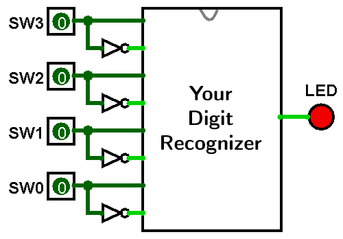
inside the Digit Recognizer count towards your total "gates used."
Only use the input NOT gates that help you simplify your design.
Task 5 – Multi-Digit Recognizer (Implementation)
Recognizing only one digit is a bit simplistic, so we’d like to scale it up to handle more digits.
- Copy your Lab 1 project folder (or unzip a fresh copy of ) into a new Lab 2 project folder.
- Download lab2.sv and lab2_tb.sv
(code) into your Lab 2 project folder, add
them to your Quartus project, and set lab2.sv as your
top-level module.
Note that we are giving you a pre-written test bench!
Note that the testbench uses an "initial" statement to generate the input patterns, with #10 delays and a for-statement. However, the testbench is non-synthesizable (i.e., the code doesn't compile to hardware and is therefore only useful/meaningful in simulation).
- In lab2.sv, implement the logic for a circuit that recognizes the last two digits of your student ID number. SW3-SW0 will be the rightmost digit, encoded as in Task 4, and SW7-SW4 will be the next digit, using a similar code (e.g., the digit 8 is encoded as SW7=1, SW6=0, SW5=0, SW4=0). Make sure to test your design in simulation BEFORE mapping it to the FPGA.
Lab Requirements
Lab Report
Due before Wednesday section, submitted as a PDF on .
- A simple, accurate explanation of what the mux4_1 circuit does. Note: We do NOT want a written description of the circuit gates, we want a description of what it actually does – if you're not sure, see how we described how the mux2_1 circuit works in Section 2 of the Quartus Tutorial.
- The value of the signal (TRUE or FALSE) that makes the LEDs light up.
- The position of the switches (up or down) that cause them to output TRUE.
- The position of the push buttons (pressed or unpressed) that cause them to output TRUE.
- A circuit diagram of your 1-digit recognizer circuit.
- A screenshot of the ModelSim simulation for your 2-digit recognizer design (always with explanation!).
- How many hours (estimated) it took to complete this lab in total, including reading, planning, designing, coding, debugging, and testing.
- Separately, upload your finished/modified code (lab1.sv, lab2.sv, and lab2_tb.sv).
Lab Demo
Due by the end of the day on Friday, but typically during your assigned demo slot or a scheduled support hour.
- Demonstrate your working simulation of the mux4_1 circuit.
- Demonstrate your working NOR and double inverter circuits.
- Explain your ModelSim simulation of your 2-digit recognizer circuit.
- Demonstrate your 2-digit recognizer working in hardware.
Grading
Working Design
90 points for correctness, style, and testing.
Logic Minimization
Up to 10 points for using as few logic gates as possible in Task 4.
Each gate (NOT, NAND, NOR) counts the same, though any NOT gates connected directly to a switch input are not counted. The fewer gates, regardless of the number of chips, the better the grade.