CPU - 32bit RISC
Introduction
I designed a experimental 32-bit RISC CPU and implemented on a Xilinx FPGA chip. An ASM program that prints prime numbers below 100 demonstrates its functionality.
Instruction Set
The 32-bit instruction set covers common DLX instructions. It is divided into three types, R-type, I-type and J-type. R-type are register instructions with three register references. I-type instructions contain two registers and a 16-bits immediate value. J-type instructions containing a 26-bit address are jumps. These instructions are coded as follows,
R-type : op(6) rs1(5) rs2(5) rd(5) func(11) I-type : op(6) rs1(5) rd(5) J-type : op(6) Since the memory on the experimental device (FD-MCES) is 32Kbytes, we can use 'BEQZ R0 label' instead of 'J label'. So there is no J-type instructions in this implementation. (Register R0 remains 0.)
Instruction classificaiton & operation-code (op):
NOP 000000 LOAD 010xxx STORE 011xxx ALU(R-type) 100xxx ALU(I-type) 11xxxx Affecting Program Flow 101xxx The detailed instruction description:INS.DEF .
Clock Signal
- Main Clock
CLK: External Clock Signal
MCLK: , to access onboard devices including RAM, printer, keyboard.
CLK_main: CPU working clock (out),
Since the onboard-RAM supports only 16-bit access, we simulate a 32-bit RAM via twice the accessing in one singal CLK_main.

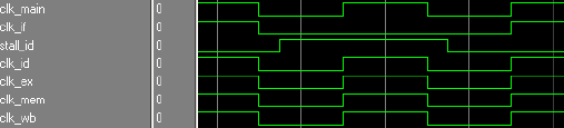
- Pipeline sub-Clocks
For the no-stall case, the pipeline subClock Signals, CLK_IF, CLK_ID, CLK_EX, CLK_MEM, CLK_WB, follows the main clock CLK_main.
For the stall case, a bubble (NOP instruction) is sent to the next stage of pipeline and all previous stages stall for a time-step.
The following shows an example, where the ID requires a freeze. Thus, its previous CLK_IF stops trigger in the current cycle,
The CPU Structure
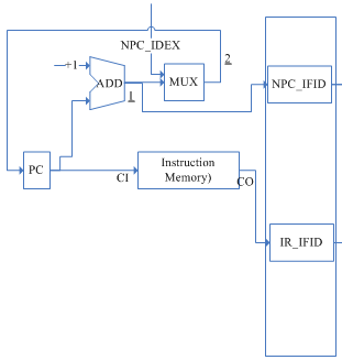
- Instruction Fetch (IF)
Set PC to FFFF when Reset = 0. Let PC+1 at each cycle, (or modify PC according to NPC_IDEX for jump).
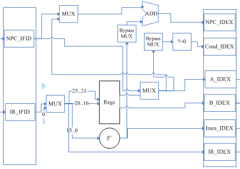
- Decode
(ID)
'Jump' is decoded in the ID stage in order to prevent possible stalling sometimes.
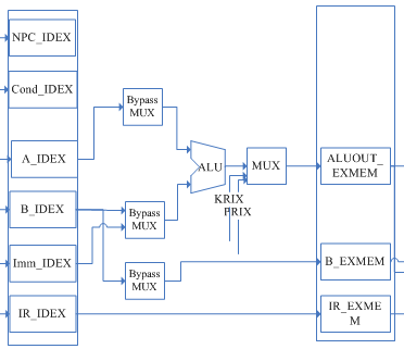
- Execute (EX)
ALU operates according to the instruction in IR_IDEX.
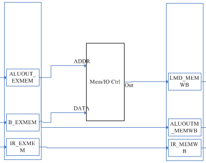
- Access (MEM)
The 'MEM/IO Ctrl' on the experimental board is the interface accessing memory and io devices. MCLK, twice the frequency of CLK_main is its clock signal. In order to simulate a 32-bit memory using the 16-bit memory on the experimental board, there are two accesses in one singal CLK_main.
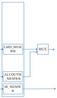
- Writeback
Instructions write their results into the registers by selecting data from LMD_MEMWB or ALUOUT_MEMWB.
Downloads
- The hardware description: CPU.VHD
- Instructions definition: INS.DEF
- The assembly source code to print prime numbers: PRIME.ASM
- The machine code: PRIME.LST
[Go to my Homepage]
Page last updated:
January 3, 2008 7:27 PM