CSE370 Assignment 4
Distributed: 14 April 2000
Due: 21 April 2000
Reading:
-
Katz, Chapter 3 revised - handout.
-
Katz, Chapter 2 textbook (pp. 65-85 and 89-91).
Exercises:
-
Exactly as one can define a real variable by an equation which needs to
be solved for the given variable (for example 2x2 + x - 2 = 0), one can
also define a boolean function by giving an equation which needs to be
solved for the unknown boolean function. For example, if S and T are given
boolean expressions, one might define the boolean function f by requiring
that S * f = T. Note that, exactly as in the real number case, there might
be more than one distinct boolean function f that solves the equation (two
solutions are said to be distinct if one cannot be derived from the other
using Boolean algebra).
Let R = (A' + C + D)(A + B + C' + D')(A' + C' + D') and S = A'C' + BC'D.
Give an expression for one possible boolean function F that satisfies the
equation R and F = S.
How many distinct solutions for f are there in this case? Explain.
-
Construct a schematic diagram for the functions that appear on slide #23
of the Combinational Logic lectures. Assign a delay of 1 to inverters,
2 to 2-inputs AND and OR gates, 4 to 3-input AND and OR gates, and 6 to
XOR gates. Use the DesignWorks simulator to create waveforms similar
to those on slide #26. Turn in a printout of the waveforms and explain
why the waveforms have the shape they have and why thy differ from those
on slide #26.
-
Factor the following sum of products experssions:
(a) AD + AE + BD + BE + CD + CE + AF
(b) AC + ADE + BC + BDE
-
Implement the 2-bit multiplier function (i.e., 2-bit number AB times 2-bit
number CD yields 4-bit number WXYZ) using 4 16:1 multiplexers. Show you
truth table and how you derived the inputs to the multiplexers. Now reimplement
the circuit using 4 8:1 multiplexers controlled by the inputs A, B, and
C (you can assume that D and D' are available). In addition to these hand-drawn
circuits, turn in a verified DesignWorks schematic that uses the Mux-8
devices in the Primlog library to implement the Y and Z outputs (make
sure to tie the EN input of the multiplexers to 0 to enable their operation
- you can use another switch for this).
-
Determine a minimal sum-of-products form for the following functions using
the appropriately sized K-maps.
(a) f(A, B, C, D) = Sm(0, 1, 4, 5, 12, 13)
(b) f(A, B, C, D) = PM(1, 3, 7, 9, 11, 15)
(c) f(A, B, C, D) = Sm(1, 7, 11, 13) + Sd(0,
5, 10, 15)
(d) f(A, B, C, D) = Sm(0, 2, 8, 9) + Sd(1,
3)
(e) f(A, B, C) = A xor B xor C
-
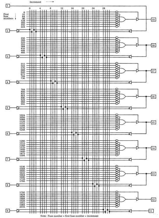
Implement the 2-bit multiplier of problem #4 using a 16H8
PAL (i.e., print out the figure and places "x"s where you want connections
made in the AND plane. Ignore the first product term in each group that
goes to the tri-state buffer (triangle) after the OR gate. Order the inputs
as A, B, C, D and the outputs as W, X, Y, Z vertically from top to bottom.
Materials:
Rationale:
-
To understand the time behavior of digital circuits.
-
To become facile with the minimization of Boolean functions using K-maps.
-
To practice mapping of Boolean functions onto regular combinational logic
structures.
Comments to: cse370-webmaster@cs.washington.edu (Last Update:
)